Double-Sided SMD PCB
Design & Manufacturing
Specialized double-sided PCB design optimized for Surface Mount Device (SMD) components, balancing performance and production efficiency.
SMD Optimization for Double-Sided Boards
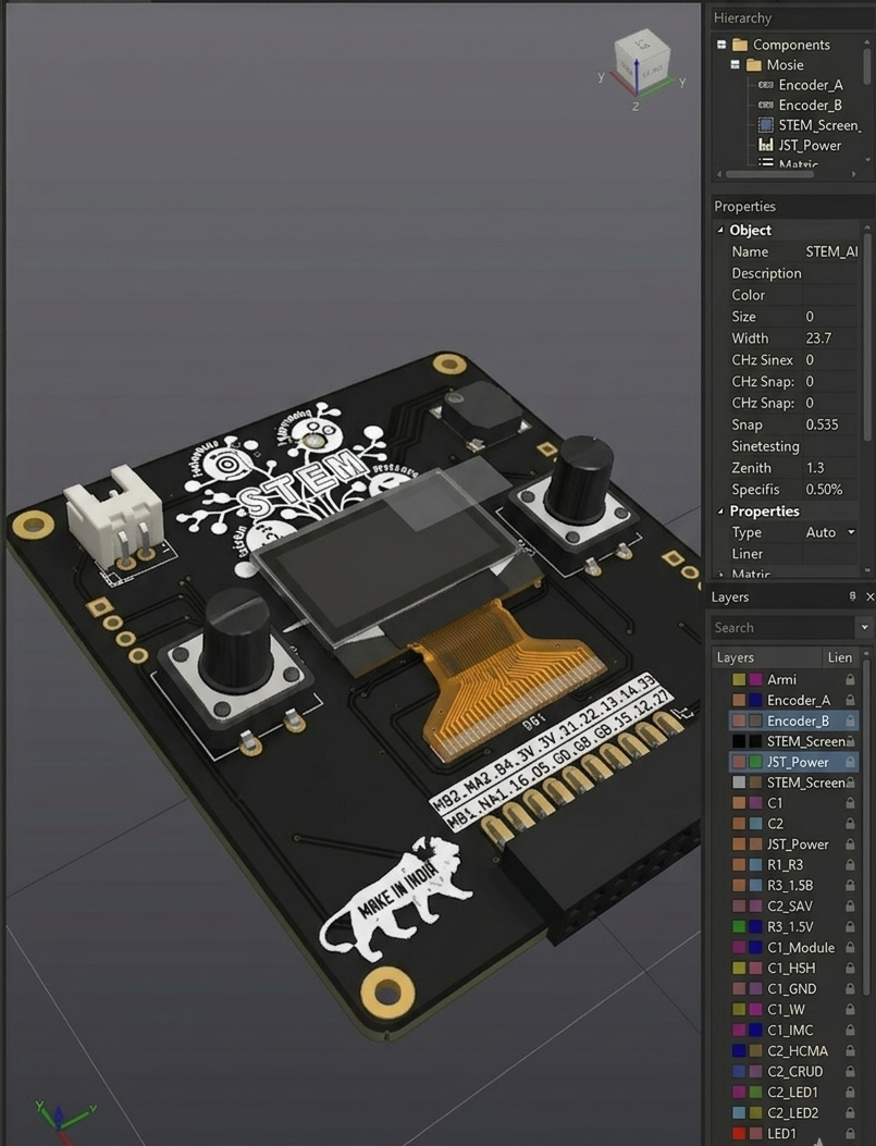
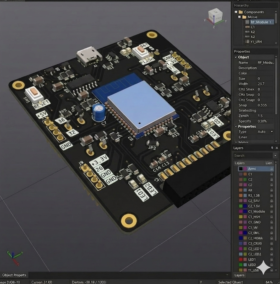
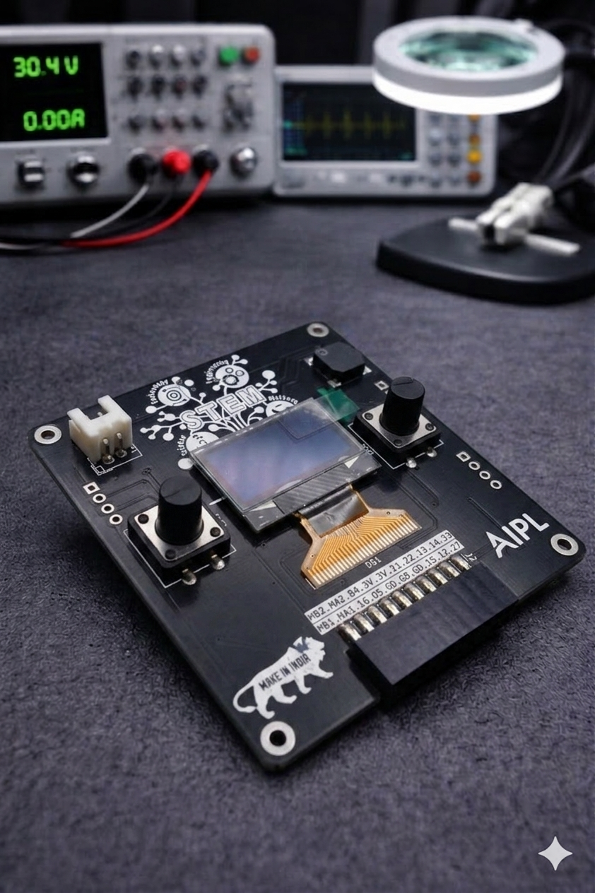
Our Double-Sided SMD PCB design leverages both top and bottom copper layers to deliver higher component density and more complex circuit routing. By utilizing SMD technology across dual conductive layers, we provide advanced compact solutions for high-performance modern electronics.
- SMD Compatibility: Precision-engineered for 0402, 0603, and fine-pitch ICs.
- Automated Assembly: Optimized for pick-and-place manufacturing.
- Thermal Management: Enhanced layouts for heat dissipation in SMD components.
SMD Technical Specifications
Engineered for Surface Mount Technology
Materials
- FR-4 High TG (Recommended for Reflow)
- CEM-3 / Aluminum Base
- Metal Core PCB (MCPCB)
- Polyimide (Flexible)
SMD Precision
- Min Pad Pitch: 0.4mm
- Solder Mask Clearance: 2 mil
- Copper Weight: 1oz - 2oz
- Profile: V-Cut / Routing
Surface Finishes
- ENIG (Highly Recommended for SMD)
- Immersion Silver / Tin
- Lead-Free HASL
- Hard Gold / ENEPIG
SMD Design Rules
- Min Trace/Space: 3/3 mil
- Via-in-Pad capable
- Solder Mask: Matte/Glossy Green, Black
- Silkscreen: High-Resolution White
SMD Focused Process
DFM Analysis
Design for Manufacturing review for SMD layout.
Stencil Fab
Laser-cut stainless steel stencils for paste.
Reflow Soldering
Controlled thermal profiles for SMD pads.
Automated AOI
Camera-based inspection of component solder.
X-Ray Test
Verification of BGA and hidden SMD joints.
Start Your SMD Project Today
Get a specialized quote for your Double-Sided SMD PCB requirements. Experience precision manufacturing tailored for high-density, dual-layer surface-mount technology.